The atom-thin sheets of graphene has inspired solar cell material to take the same form, says S.Ananthanarayanan.
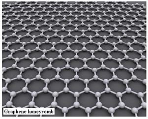
Graphene is a form of carbon that shows crystal structure in two dimensions and displays remarkable mechanical, electrical and optical properties. But for all that, it cannot be used as a solar cell material, because the disposition of the carbon atoms in graphene is not suited to emit electrons when excited by light radiation. On the other hand, the element silicon is suited for solar cells, but silicon wafers are bulky, rigid and opaque.
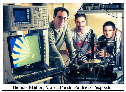
Andreas Pospischil, Marco M. Furchi and Thomas Mueller, at the School of Photonics at Vienna University report in Nature Nanotechnology that atoms of tungsten and selenium combine to form graphene-like, ultra-thin layers and the layers of these elements also display photo-voltaic properties. The material, tungsten diselenide, appears to have come of age, because the same issue of Nature Nanotechnology carries two more reports, one from Britton W. H. Baugher, Hugh O. H. Churchill, Yafang Yang and Pablo Jarillo-Herrero, from MIT and another from Jason S. Ross, Philip Klement, Aaron M. Jones, Nirmal J. Ghimire, Jiaqiang Yan, D. G. Mandrus, Takashi Taniguchi, Kenji Watanabe, Kenji Kitamura, Wang Yao, David H. Cobden and Xiaodong Xu1, from Washington, Tennessee, Germany, Japan and China and both reports are of essentially the same application.
The properties of graphene arise because of the electronic structure of the carbon atom, which has four electrons in the outermost electron shell. It is this electronic structure that gives the carbon atom itself its versatility. As atoms tend to combine so that they have stable, eight electron outer shell, carbon atoms can form bonds with four adjacent atoms that have an electron to spare, and the adjacent atoms can well be other carbon atoms. Carbon thus forms the extremely hard diamond crystal, where carbon atoms lock all four bonds in a three dimensional lattice, or a soft form where carbon atoms make only three bonds, in the form of sheets made up of hexagons, the ‘honeycomb lattice’. This second form is graphite, where the sheets are stacked with feeble binding forces and the sheets easily slide over one another. This two dimensional form is unique to carbon and single sheets are now realized as graphene. Diamond is great for mechanical strength, but graphene, with its unused bond, is a good conducor.
But the property of putting out electrons when exited by light is a different property, more common at the surface of metals, where the outermost electrons of the atoms are relatively less strongly bound. In such cases, photons of light can knock some of these outer shell electrons free of the mother atoms, leaving them free to move, so long as they do not meet an atom which has lost an electron,, when the free electron recombines. Some materials can be treated with impurities, the atoms of which have either one more or one less outer electron., and when excited by light, what is set free is either an electron, or a ‘lack of an electron’ which is called a ‘hole’ If there is a junction of these two kinds of material, then the free electrons can cross over, but not the holes, and the sides get oppositely charged, which means the electrons would flow through a conductor, to go back to the other side, and we would have a photo-cell. The element silicon happens to be one such. It has the correct forces holding down the peripheral electrons, which helps it react to light, and also a carbon-like crystal structure, which helps create conditions to harvest electricity. But, as we have noted, silicon is bulky, rigid and opaque, and also expensive.
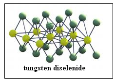
An alternative material of promise has been tungsten biselenide, where an atom of tungsten forms a chemical bond with two atoms of selenium. Tungsten is a metal which is able to participate in forming bonds with the help of as many as six peripheral electrons. Selenium can also from bonds by accepting or sharing different numbers of electrons. When tungsten biselenide forms crystals, it turns out that the stable form is a sheet, of a layer of tungsten atoms sandwiched between two layers of selenium atoms. This is also a very thin sheet, like the sheet of graphene, and it shares the properties of transparence and flexibility
The three groups of researchers featured in Nature Nanotechnology have worked on tungsten bislenide sheets and by proper doping of crystals with impurities, have brought about the conditions of electrons, which are pumped out when a junction is exposed to light, piling up on one side, which would drive a current.
The experimenters demonstrate that the material can be used to efficiently generate a current when exposed to light, or to change the junction from conducting to non conducting, by turning a beam of light on or off and also to make the junction emit light when a current is passed. These properties would enable the device to work as a photocell, as a switch or as a display system. As the material is light and flexible, it could be mounted anywhere and in any shape. As the material is transparent, it would allow the bulk of the light falling on it to pass through, at the same time generating electricity from a small part that it absorbs. More layers could be used to block more light and generate more power.
When used as a switch, the beam of light that activates the switch could also signal the state of the switch, by illuminating the relevant signboard. And when used as display, the image would appear on a transparent screen, that is, without blocking the view. Digital information in a rapidly fluctuating light beam could be used to drive a switch which would imprint the signal on to a current. Alternately an electrical digital signal could be converted into an optical signal.
With rapid advances in production of two dimensional crystals, in bulk and at low cost, these applications would profoundly impact “future developments in solar, lighting and display technologies,” say the authors of the first paper cited.
' ------------------------------------------------------------------------------------------
Do respond to : response@simplescience.in