You cannot get more nano than down to the level of atoms, says S.Ananthanarayanan.
Miniaturisation was at first the progress of finer and finer workmanship, like wrist watches, or model ships, or desk-top size working versions of the steam locomotive. The integrated circuit or the microchip, where thousands of electronic components fit on a sliver the size of a postage stamp, is perhaps the ultimate leap forward. But nano-technology uses crystal structure of materials and the bulk behavior of groups of atoms to create devices that cannot be assembled manually.
If we go further and work at the level of individual atoms themselves, we are usually in the domain of chemistry and we create new compounds, not atoms–size devices. Just short of this may be working with assemblies of atoms in sheets which are just one atom thick. This is what Chul-Ho Lee, Gwan-Hyoung Lee, Arend M. van der Zande, Wenchao Chen, Yilei Li, Minyong Han, Xu Cui, Ghidewon Arefe, Colin Nuckolls, Tony F. Heinz, Jing Guo, James Hone and Philip Kim, from Korea University and Yonsei University at Seoul and at Columbia and University of Florida report in their paper in the journal, Nature Nanotechnology.
One atom thick
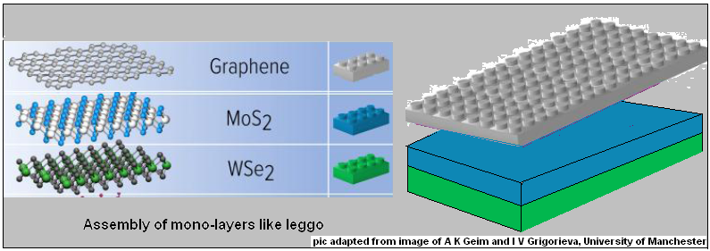
Atoms are 3-dimensional things, with a nucleus surrounded by electrons in shells, and shaped more like a ball, than like a plate. Atoms, or even groups of atoms, like compounds, hence usually form bonds, using the outer electrons, with other atoms or compounds, in 3 dimensions. Or, even if they lay themselves out, in small groups, as a sheet, they strongly influence other atoms on either side of the sheet, which loses a purely 2-dimensional character. But there are elements, like carbon, which form very stable 3-D crystals, like the diamond, but can also keep all bonds within one plane and form extended sheets that freely slide over one another. Graphite is the classic example and it is the property of sheets sliding smoothly that is used to make marks on paper, when graphite is used in pencil lead. But the main thing about this structure is that the sheets of atoms, which slide over other sheets, in this case called, graphene, are each only one atom thick. Graphene, or other similar forms of carbon, in the form of nano-tubes, or balls in a geodesic dome structure, also have interesting electrical properties, with prospects of application as connectors in micro-electronics.
The bonds between atoms, in the 2-D, sheet structure. are because of exchange or sharing of electrons and these are stable and strong, in fact, very strong. But between two adjacent layers of this kind, there are no electronic bonds, but just a mild attraction, like the forces between neutral atoms in a gas, which tend to slightly reduce the pressure the speed of the gas molecules exert on the walls of a container. These forces are called van der Waals forces and materials that consist of one-atom layers held together by such forces are van der Waals materials.
While graphene was the first such material, which forms mono-layers, as the structure was called, that was studied, attention in the last few years has moved to other materials. The material of interest is a category of compounds contain atoms of metals that have unfilled inner shells in their electronic structure, which allows them to form a plurality of kinds of links with other atoms. These atoms combine with atoms of elements of the class of sulphur, selenium, tellurium. These later elements, which are like oxygen, need, for stability, to form a pair of bonds with the atoms of the metal with which they combine. The result is that in these compounds, the electronic structure and the masses are suitable for mutual combination in the form of a mat, or a sheet, where all bonds are satisfied along a single plane and there is no need to seek bonds in the 3rd dimension, for stability.
These other materials, hence, also form mono-layers, like graphene. But in these materials, where there is more complexity in the structure of the monolayer sheet, it is possible control how they conduct electricity, in the way that can be done with bulk silicon, which is the basis of semiconductor technology, diodes, transistors, and all of modern electronics. Specifically, these materials could be insulators in the pure form, but become conductors, called semiconductors, if some of the atoms in their structure were replaced by others, which have one more or one less outer electron in their electronic structure. These newcomers then land up with either one extra electron, or with a ‘gap’ where there should have been an electron. And this anomaly, of an extra or a missing electron, is free; in the assemblage, to carry an electric current. If there is a junction, of these two kinds of conducting materials, then, we have a case where the ‘extra’ electrons can cross over, but there is no way a ‘gap’ can cross, which means the junction is a one way gate for an electric current. It is with such junctions that electronic circuits can allow or prevent the passage of a current, a property that is used to record data, carry out calculations, and the other wonders of electronics.
Not only can junctions of composite monolayers be bestowed with semiconductor properties, they can be even be tweaked to respond to light. The response can be to change from insulator to conductor, the other way about, for use as light operated switch, or to throw out electrons and develop a charge, for use as a detector. Inversely, the junctions can emit photons when charged with electricity, which would enable their use in display. Different compositions of the monolayer material would lead to different levels of response, and the response could even be controlled by using external electric or magnetic fields.
Another feature of these monolayer junctions is that interface of two layers is of a pair of layers that are smooth at the atoms level and when placed in contact, they are linked by van der Waals’ forces. This ensures a high quality interface, without the limitations inherent in conventional fabrication and the structure created is fundamentally different and more flexible.
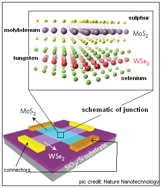
The authors of the paper in Nature Nanomaterials report that they used a mono-layer of tungsten diselenide (WSe2) as the layer with the ‘gaps’ or the holes and a mono-layer of molybdenum disulphide (MoS2) as the layer with free electrons, to create the junction of the two kinds of semiconductors. The two mono-layers consist of a hexagonally packed layer of tungsten or molybdenum atoms, sandwiched between two planes of selenium or sulphur atoms, as the case may be.
The mono-layers were deposited, in contact by van der Waals forces, on a silica/silicon base and the layers were provided with electrical contacts. The base was also charged, as this charge affects the density of available current carriers, that is, the holes or the electrons, in the mono-layers. Trials then showed that the junction worked effectively as a one-way gate for an electric current, and the current flowing could be controlled by the charge applied to the base. Further trials with exposure of the junction to white light or light of specific colours again showed that the mono-layers were induced to emit electrons, which, naturally, had to flow in one direction only and hence charge one side of the junction, like in a normal photocell. To improve the collection of the photocurrent, the junction was also sandwiched between mono-layers of graphene.
Analyses of the response of the junction to the different parameters shows that the mechanism of working in mono-atomic layers is fundamentally different from conventional devices. But the work represents a first creation of atomically thin junction of semiconductor layers which “will lead to unique material platforms for novel, high-performance electronic and optoelectronic devices,” the authors say.
Do respond to : response@simplescience.in
