The award of the Nobel Prizes of 2014 for physics and chemistry to work in the field of photonics seems to be well timed, says S.Ananthanarayanan.
The United Nations have proclaimed 2015 as the International Year of Light. The objective is to raise awareness of the achievements of light science and its applications, and its importance to humankind. Different stakeholders, including UNESCO, scientific societies and unions, educational and research institutions, technology platforms, non-profit organizations and private sector partners are coming together to promote and celebrate the significance of light and its applications during 2015.
Almost to bring in the year, the Royal Swedish Academy of Sciences, in October 2014, has selected two groups of inventors, who made a breakthrough in ‘efficient light emitting diodes’ and ‘super resolved fluorescence microscopy’, both areas in the field of light technologies, for the Nobel Prize in physics and chemistry, respectively.
Physics
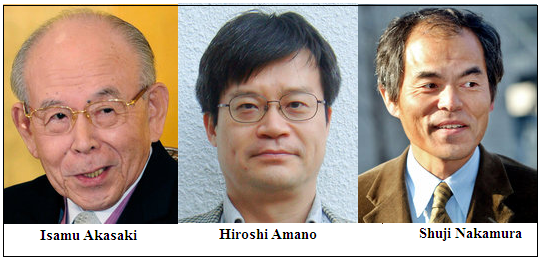
The prize has gone to Japanese scientists, Isamu Akasaki, Hiroshi Amano and Shuji Nakamura for their work in extending light emitting devices, called diodes, to efficiently shine in the blue region of the spectrum, which enabled a group of such devices to create white light. The early light emitting diodes, or LEDs, were a great step forward from the previous technology of liquid crystal display, or LCD, but their use was limited because devices that gave off blue light had not been developed.
The earliest device used for display was TV tube, also called the Cathode Ray Tube, which was an electron beam that struck a screen coated with chemicals. The electron beam was made to scan the whole screen several times a second and the strength of the beam varied as it moved, to create bright or dark spots, which formed the display. The trouble was that this device needed high voltage to create the electron beam and was bulky. The coating on the screen was also poisonous and difficult to dispose of.
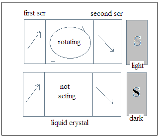
The Liquid Crystal display (LCD) consisted of an array of small devices that could be light or dark, depending on voltages applied to each of them. Each LCD cell was actually a window that opened or shut, according to the voltage applied, and consisted of a pair of transparent, but conducting screens, with a property of allowing only light in which the vibrations were in a particular plane to pass. The screens were separated by a material, the liquid crystal, which rotated the plane of vibration of light coming through the first screen before it struck the second screen. And this second screen was oriented so that in the normal course, the light passed this screen also and the cell appeared grey. But when a voltage was applied across the two screens, which were conducting, the liquid crystal stopped turning the plane of vibration of light and light did not pass through the second screen. The cell then appeared dark. The devices worked with very low currents and could be made small enough so the array could display reasonably clear images.
LCDs were succeeded by the Light emitting diode (LED), which made for much finer grain of images and faster switching on or off, better power efficiency and longer life. The LEDs were tiny specks of crystals consisting of atoms, which had not just few electrons to allow less current to pass, like an insulator, but were also without free electrons that allow currents readily, as in conductors. Now, this class, known as semiconductors, can be modified, by adding an impurity, so that they have either a few extra electrons which carry current, or a few places which lack an electron, called holes, which can also carry current in the opposite way. If there is a junction of these two kinds of semiconductor, the free electrons on one side drift into the other side, to combine with holes, but also create a charge difference by moving about, and the movement stops. But if a voltage is applied, which keeps the current going, the instances of electrons combining with holes gives off some energy, which can be flashes of light. Such devices can then be displays or even light sources for communication, and they are a great step forward in efficiency.
The colour of the light emitted can also be changed by varying the materials, and strong emitters in a number of colours, which could be combined, have been developed. But for creating white light, it was necessary to have a source of the blue component too, and developing a good source of this colour did not succeed for a long time.
The achievement of the three Japanese Nobel laureates was to work on the energy difference when electrons fell into holes in different materials and then to overcome the problems in creating defect-free crystals of the best material – finally to arrive at Gallium Nitride, and a method to grow the crystals and then to dope them with the right impurities. Development of an efficient LED source of blue light has enabled a new generation of image displays and also highly energy efficient white light sources for daily lighting.
Chemistry
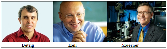
The Prize for chemistry goes to Eric Betzig, Virginia, Stefan Hell, Gottingen, Germany and W. E. Moerner, Stanford University, for their independent work in developing very high resolution microscopy which uses a molecular property called fluorescence.
Normal microscopy has a natural limit to how good it can get, and this limit is imposed by the frequency of the light used, the medium through which the light passes and the diameter of the microscope lens. Using high frequency light for high resolution would destroy the samples and there are physical limits to the size of lenses. But in floursescence, the emission of light is by single molecules within the sample being studied, and each molecule is a point source. When observing a point source, the limitations of frequency of light and the size of the lens can be compensated by observing a greater number of photons, which can be done in fluorescence by making a large number of observations, or by recording the fluorescence for a long time.
The first successful sensing of single molecules using light was reported by W.E. Moerner, along with a colleague, in 1989. Soon after, in 1992, Eric Betzig discovered a method of positioning a sub wavelength-size hole in a metal screen at the tip of an optical fibre and exciting single molecule fluorescence.
Stefan Hell worked on another way to increase resolution, which takes off from observing fluorescence where the emission is not of one photon at a time, but of two or more. This method increases resolution by a factor that depends on the number of photons, but its implementation is nearly impossible. Hell used a device of suppressing fluorescence in a doughnut shaped area and shrinking the hole of the doughnut, a method that mimics high intensity emission and hence high resolution. The use of this method, with intense emitters of fluorescence, has been able to reach resolution as low as 10 nanometers.
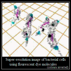
With a further refinement of using statistical methods to resolve single molecule events from among others, the recent progress in this field of optical nanoscopy has been breathtaking. Not only has imaging below the limit set by the wavelength of light become possible, but a variety of applications has helped push back the frontier of our understanding of matter at the very small scale.
Do respond to : response@simplescience.in
------------------------------------------------------------------------------------------
